(China (Mainland))


Product Summary
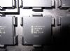
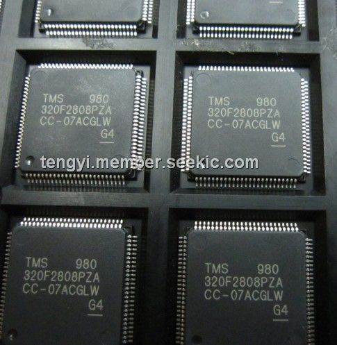
The TMS320F280PZA is a DSP. The device is a highly integrated, high-performance solution for demanding control applications.
Parametrics
TMS320F280PZA absolute maximum ratings: (1)Supply voltage range, V DDIO, V DD3VFL with respect to V SS: - 0.3 V to 4.6 V; (2)Supply voltage range, V DDA2, V DDAIO with respect to V SSA: - 0.3 V to 4.6 V; (3)Supply voltage range, V DD with respect to V SS: - 0.3 V to 2.5 V; (4)Supply voltage range, V DD1A18, V DD2A18 with respect to V SSA: - 0.3 V to 2.5 V; (5)Supply voltage range, V SSA2, V SSAIO, V SS1AGND, V SS2AGND with respect to V SS: - 0.3 V to 0.3 V; (6)Input voltage range, V IN: - 0.3 V to 4.6 V; (7)Output voltage range, V O: - 0.3 V to 4.6 V; (8)Input clamp current, I IK (V IN < 0 or V IN > V DDIO ): ± 20 mA; (9)Output clamp current, I OK (V O < 0 or V O > V DDIO ): ± 20 mA; (10)Operating ambient temperature ranges, T A: A version (GGM, PZ): - 40 to 85℃.
Features
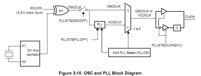
TMS320F280PZA features: (1)Internal or External Reference; (2)Up to 35 Individually Programmable, Multiplexed GPIO Pins With Input Filtering; (3)Analysis and Breakpoint Functions; (4)Real-Time Debug via Hardware; (5)Low-Power Modes and Power Savings; (6)IDLE, STANDBY, HALT Modes Supported; (7)Disable Individual Peripheral Clocks; (8)Package Options: Thin Quad Flatpack (PZ); MicroStar BGA (GGM, ZGM); (9)Watchdog Timer Module; (10)Any GPIO A Pin Can Be Connected to One of the Three External Core Interrupts; (11)Peripheral Interrupt Expansion (PIE) Block That Supports All 43 Peripheral Interrupts.
Diagrams
 |
 TMS3112 |
Other |
|
Data Sheet |
Negotiable |
|
||||
|
TMS3121 |
Other |
|
Data Sheet |
Negotiable |
|
||||
|
TMS320 |
Other |
|
Data Sheet |
Negotiable |
|
||||
|
TMS32010 |
Other |
|
Data Sheet |
Negotiable |
|
||||
|
TMS320AV7110 |
Other |
|
Data Sheet |
Negotiable |
|
||||
 |
TMS320BC51PQ100 |
Texas Instruments |
Digital Signal Processors & Controllers (DSP, DSC) TMS320C51PQ - 132QFP - 100MHZ/BOOT CODE |
Data Sheet |
Negotiable |
|
||||